Study for trilayer antireflection coating using dip coating technique
[State Zhejiang University, Hangzhou 310027, China]
[Abstract]We report a new structure for broadband antireflection coating by dip-coating technique, which has minimal cost and is compatible with large-scale manufacturing. The coatings are prepared by depositing SiO2 sol-gel film on a glass substrate, subsequently depositing SiO2 single-layer particle coating through electrostatic attraction, and depositing a final very thin SiO2 sol-gel film to improve the mechanical strength of the whole coating structure. The refractive index of the structure changes gradually from the top to the substrate. The transmittance of a glass substrate has been experimentally found to be improved in the spectral range of 400-1,400 nm and in the incidence angle range from 0◦ to at least 45◦. The mechanical strength is immensely improved because of the additional thin SiO2 sol-gel layer. The surface texture can be applied to the substrates of different materials and shapes as an add-on coating.
Antireflection coating, one of the most extensive research subjects in thin film optics, plays a well established role in various applications such as display panels, solar cells, and optical lenses. A perfect Antireflection coating could eliminate the reflection completely from the interface between two media for all wavelengths, polarizations, and angles of incidence. Theoretically, there are three main types of nonabsorbing omni-AR structures: single quarter-wavelength film, graded index (GRIN) structure, and textured surface antireflection structure.
For GRIN Antireflection structure, the refractive index of the structure changes gradually from the top layer to the bottom so as to yield omnidirectional and broadband Antireflection characteristics. The major challenges for this approach are the availability of materials with suitable refractive index and the mechanical properties of the coating structure, hindering such structure from practical applications. Textured structure provides another feasible solution for antireflection coating. The most successful example for textured surface is anisotropically etched pyramids on single-crystalline silicon (100) surface. Low reflectance over a wide spectral range can be achieved by anisotropic etching; however, anisotropic etching is too unreliable, and photolithography-defined surface textures are too expensive. Another simple method of obtaining textured surface is the self-assembly technique; a series of papers has been published on this bottom-up process.
Microscale surface texture can significantly reduce effective index. Low reflectance can be achieved by index matching of the surface texture to substrates with different indices. However, to the best of our knowledge, few people have considered combining the GRIN and textured surface structures.
In this letter, a novel solution-based three-layer broadband Antireflection coating that combines the methods of GRIN and textured surface structures is demonstrated. The experimental results reveal that a broadband (400−1,100nm) Antireflection coating with an average reflectance lower than 2% on one side of glass could be obtained through optimizing the optical constants of each layer. The outer SiO2 layer greatly enhances the mechanical property. Details of the fabrication process and efficiency improvement are described.
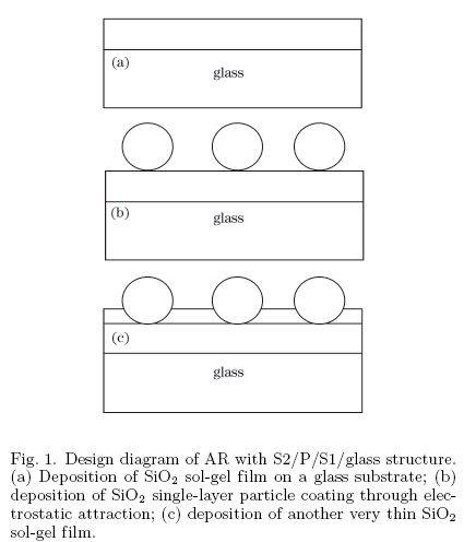
Figure 1 shows the design diagram of our antireflection coating with S2/P/S1/glass structure. The S1 layer is a dip coated SiO2 film on glass substrate serving as the GRIN structure. The P layer, which serves as the textured surface structure, is a self-assembled spherical SiO2 colloidal layer using electrostatic self-assembly method. An additional thin SiO2 porous layer (S2) is the outer layer of the AR structure, which serves as a “glue” to hold together and anchor the silica particles. The size of SiO2 particles and the thickness of the S1 layer were optimized by our software based on rigorous coupled-wave analysis.
Solutions for sol-gel dip-coating were prepared based on a metal alkoxide precursor, tetraethyl orthosilicate (TEOS, Si(C2H5O)4). For the preparation of a solution suitable for SiO2 deposition, TEOS was hydrolyzed in the presence of hydrochloric acid and deionized water. The SiO2 film for S1 layer was dip-coated on the glass surface from such solution at 100−400 mm/min. The solution for S2 layer was diluted 50 times from the aforementioned solution. The desired film thickness could be adjusted in the range of 20−80 nm by controlling dip speed. Each layer was annealed at 350 ◦C for 30 min.
Electrostatic attraction is a useful interaction for assembling materials such as polyelectrolytes and charged colloidal particles. Commercially available poly(diallyldimethylammonium) (PDDA, Aldrich, medium MW,20 wt.-%) and monodisperse SiO2 colloid solution (0.1-μm particle, 30% in ethylene glycol, Alfa Aesar) were used without further purification. PDDA was diluted to a concentration of 4 mg/ml. The SiO2 colloid solution was diluted to provide concentrations of 10 mg/ml (pH 9). The colloidal SiO2 particles are negatively charged in this solution because the point of zero charged is 2.1 for SiO2. Moreover, PDDA is a linear quaternary ammonium polycation. The rinsed substrates were dipped in PDDA solution for 5 min, with intermediate water washing, and then dipped in SiO2 colloid solution for another 5 min, followed by extensive washing with deionized water. The SiO2 particles were deposited onto the polymer layer. The particle layer was annealed at 350 ◦C for 10 min to remove the PDDA. This procedure is similar to that used by Hattori for the preparation of SiO2 particlebased Antireflection coating.
The refractive index and thickness of S1 film were calculated by fitting the reflectance of the film in the wavelength region of 400−780 nm. After the dip coating and annealing process, the reflectance of the film was measured using a spectrophotometer in the wavelength region of λ = 380−780 nm (Olympus, USPM-RU), whereas the transmittance of the film was measured with a scanning spectrophotometer in the wavelength region of 400−1,400 nm (Shimadzu, UV-VIS-NIR). Because of limitations in the setup, the reflectance of a singlesided Antireflection coating was measured. Surface morphology and cross sections of the coating were examined with a scanning electron microscope (SEM, Zeiss, ULTRA 55). The scratch resistance of the coating was tested using Floch’s method. A piece of thin blotting paper soaked in ethanol was used to rub the coating 10 times. Meanwhile, an adhesive tape test was conducted by laying the tape across the coated surface vigorously and then quickly pulling it away from the coating at an angle of approximately 45◦. Then, the interference color of the coating was observed to measure the mechanical property.
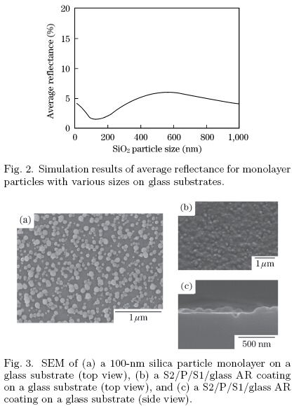
Some simulation results were encouraging. The simulation is based on rigorous coupled-wave analysis, which includes both transverse-electric and transverse-magnetic polarizations. The average reflectance covering the whole wavelength region from 400 to 1,400 nm of the single P layer as a function of the particle size is shown in Fig.2 in normal incidence. It was evaluated by performing the integration of wavelength. The packing density of SiO2 particles has almost no effect on the total reflectivity;thus, only the close-packed structure was simulated.
Good performance can be achieved when the size of the particle is 100 nm based on the simulated results.Figure 3(a) shows electron micrographs of a monolayer of 100-nm spherical silica particles coated onto a glass substrate. The coating is a monolayer of the particles with random distribution. Figure 3(b) illustrates a scanning electron microscope (SEM) top view of the S2/P/S1 structure on a glass substrate. The particles were embedded in the thin film S2. Figure 3(c) shows the cross section of a glass coated with the S2/P/S1 structure.
Figure 4 shows a normal-incidence transmittance measurement of a glass substrate with the described Antireflection coating. The oscillation around λ = 850 nm of the transmittance spectra is due to alternation for the light source of our spectrophotometer. For comparison, the transmittance spectra of bare glass substrate were also measured. The spherical surface coating covering both sides of the substrate improved the transmittance from ∼91.5% to 94.7% around λ = 500 nm.
Before depositing the particles, a sol-gel thin film of SiO2 was dip-coated onto glass. The refractive index of the deposited film (i.e., 1.45 at 500 nm) was obtained by fitting the reflectance spectra with the thickness of the film. The absorption of this S1 film was not considered in the experiment because it will not affect the reflectivity results significantly. The AR properties with P/S1/glass structure were found to be greatly improved, as shown in Fig. 4. The transmittance of the sample with doublesided coating improved from 94.5% to 97.2% around λ = 500 nm, and from 93.5% to 94.5% around λ = 1200 nm compared with the one with P layer only. Because the refractive index of amorphous silica was 1.46, the roughly estimated refractive index of the P layer can be 1.24. The refractive index of a thin, low-iron soda lime glass was 1.53. The refractive index of air/P/S1/glass structure gradually was evidently decreased from substrate to air. The reduction in reflectivity was provided with index matching of the AR structure to substrates with index of S2. Meanwhile, the thickness effect of the sol-gel film was also investigated, as shown in Fig. 5, with the thickness of S1 equal to 20, 40, 60, and 80 nm. The best performance was achieved when the thickness of S1 was 40 nm with smooth reflectance curve. For thicker S1, the interference effect can be clearly observed.
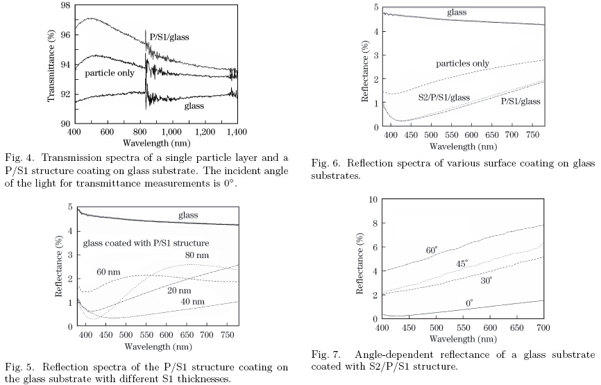
Although the P/S1 structure has excellent AR properties, the particle layer is actually easy to wipe off, even if the particles are fritted together by annealing process. The poor mechanical properties of this Antireflection structure immensely limit its practical applications. Therefore, an additional thin film S2 is needed to serve as a glue to hold together the coatings. Here, the adhesion of the S2/P/S1 coating was measured qualitatively with the tape and rubber tests. The mechanical property of the coating was shown to be improved by S2 film because the coating was unaffected by the tape and rubber tests. For comparison, the reflectance of a P/S1/glass structure, a S2/P/S1/glass structure, and a monolayer of 100-nm spherical silica particles were measured, as shown in Fig.6. Because the film S2 was very thin (approximately 10 nm), the effect on AR properties was very small.
Light scattering could not be excluded because nanoparticles were used. For P/glass structure coating, the maximum transmittance in Fig. 4 amounts to 94.8%; thus, the corrected reflectance of single side coating was estimated to be 2.6% if the particles did not introduce any absorption. Although the measured reflectance of the coating in Fig. 6 amounts to 1.4%, the light scattering would account for 2.6%−1.4%, that is 1.2%. For P/S1/glass structure coating, the maximum transmittance amounted to 97%, whereas the measured reflectance of the coating is 0.4%; the light scattering accounts for 1.1%. The light scattering caused by a single nanoparticle layer is estimated to be 1.1%.
A desirable feature of any Antireflection structure for most optical devices is omnidirectionality (i.e., the Antireflection is independent of incident angle). It is particularly important for solar cell industry because it can eliminate the need for a mechanical tracking device. Omnidirectionality can easily be accomplished with the structure of S2/P/S1 because of the layer of spherical particles. Figure 7 is an incident angle dependent reflectance measurement for the S2/P/S1 structure on a glass substrate. The S2/P/S1/glass structure coating was found to still have superior Antireflection properties at incident angles of 30◦ and 45◦.
In conclusion, a new solution-based process combining GRIN and textured surface structure is developed. This new process is compatible with large-scale manufacturing and suitable for different types of substrates because it is a low-cost and energy-efficient process with no complicated large vacuum system. The coating is prepared by depositing a sol-gel dip-coated SiO2 film, a single silica particle layer, and an additional thin SiO2 film. The low reflectance from this coating becomes omnidirectional when the particle layer is added. A broadband (400– 1,100 nm) Antireflection with the average reflection lower than 1% on glass could be obtained. The mechanical properties are immensely improved from the additional thin SiO2 sol-gel film.
 D5 Creation
Comments are Closed